- 您现在的位置:买卖IC网 > Sheet目录3880 > PIC16F785-I/SO (Microchip Technology)IC PIC MCU FLASH 2KX14 20SOIC
102
8272E–AVR–04/2013
ATmega164A/PA/324A/PA/644A/PA/1284/P
one allows the OC0A pin to toggle on Compare Matches if the WGM02 bit is set. This option is
not available for the OC0B pin (See Table 15-4 on page 105). The actual OC0x value will only
be visible on the port pin if the data direction for the port pin is set as output. The PWM wave-
form is generated by clearing (or setting) the OC0x Register at the Compare Match between
OCR0x and TCNT0 when the counter increments, and setting (or clearing) the OC0x Register at
Compare Match between OCR0x and TCNT0 when the counter decrements. The PWM fre-
quency for the output when using phase correct PWM can be calculated by the following
equation:
The N variable represents the prescale factor (1, 8, 64, 256, or 1024).
The extreme values for the OCR0A Register represent special cases when generating a PWM
waveform output in the phase correct PWM mode. If the OCR0A is set equal to BOTTOM, the
output will be continuously low and if set equal to MAX the output will be continuously high for
non-inverted PWM mode. For inverted PWM the output will have the opposite logic values.
At the very start of period 2 in Figure 15-7 OCnx has a transition from high to low even though
there is no Compare Match. The point of this transition is to guarantee symmetry around BOT-
TOM. There are two cases that give a transition without Compare Match.
OCR0A changes its value from MAX, like in Figure 15-7. When the OCR0A value is MAX the
OCn pin value is the same as the result of a down-counting Compare Match. To ensure
symmetry around BOTTOM the OCn value at MAX must correspond to the result of an up-
counting Compare Match.
The timer starts counting from a value higher than the one in OCR0A, and for that reason
misses the Compare Match and hence the OCn change that would have happened on the way
up.
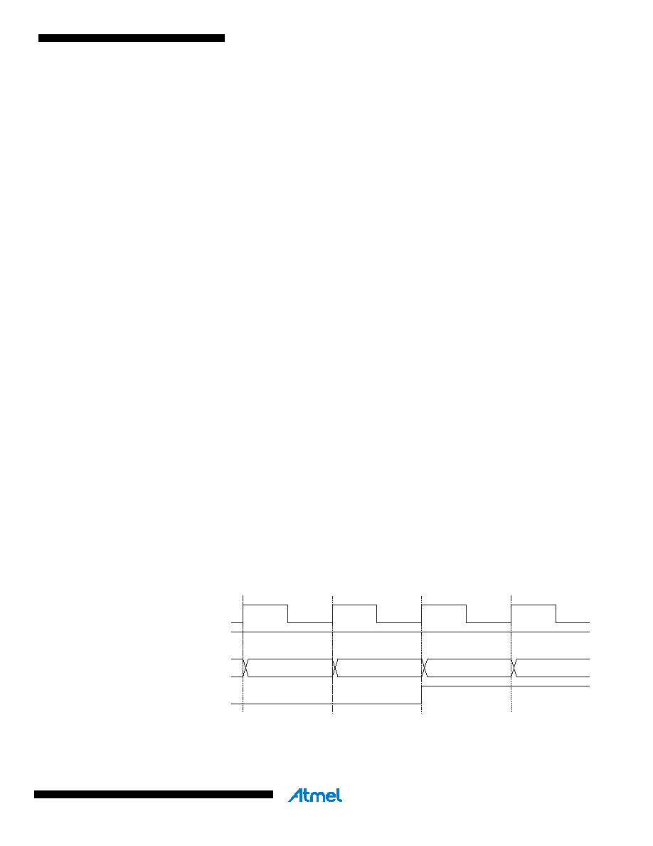
15.8
Timer/Counter Timing diagrams
The Timer/Counter is a synchronous design and the timer clock (clk
T0) is therefore shown as a
clock enable signal in the following figures. The figures include information on when Interrupt
Flags are set. Figure 15-8 contains timing data for basic Timer/Counter operation. The figure
shows the count sequence close to the MAX value in all modes other than phase correct PWM
mode.
Figure 15-8. Timer/Counter Timing diagram, no prescaling.
Figure 15-9 on page 103 shows the same timing data, but with the prescaler enabled.
f
OCnxPCPWM
f
clk_I/O
N 510
------------------
=
clk
Tn
(clk
I/O/1)
TOVn
clk
I/O
TCNTn
MAX - 1
MAX
BOTTOM
BOTTOM + 1
发布紧急采购,3分钟左右您将得到回复。
相关PDF资料
PIC16C56A-04/SO
IC MCU OTP 1KX12 18SOIC
PIC18F23K20-I/MV
IC MCU 8BIT 8KB FLASH 28UQFN
PIC16F627A-I/P
IC MCU FLASH 1KX14 EEPROM 18DIP
XF2G-1414-11
CONN FPC 14POS 0.5MM SMT
PIC16F777T-I/ML
IC PIC MCU FLASH 8KX14 44QFN
PIC18F2539T-E/SO
IC PIC MCU FLASH 12KX16 28SOIC
PIC16LF1936-I/SO
IC PIC MCU FLASH 512KX14 28-SOIC
PIC16F873AT-E/ML
IC PIC MCU FLASH 4KX14 28QFN
相关代理商/技术参数
PIC16F785-I/SS
功能描述:8位微控制器 -MCU 3.5KB FL 128R 18 I/O RoHS:否 制造商:Silicon Labs 核心:8051 处理器系列:C8051F39x 数据总线宽度:8 bit 最大时钟频率:50 MHz 程序存储器大小:16 KB 数据 RAM 大小:1 KB 片上 ADC:Yes 工作电源电压:1.8 V to 3.6 V 工作温度范围:- 40 C to + 105 C 封装 / 箱体:QFN-20 安装风格:SMD/SMT
PIC16F785T-E/SS
功能描述:8位微控制器 -MCU 3.5KB FL 128R 18 I/O RoHS:否 制造商:Silicon Labs 核心:8051 处理器系列:C8051F39x 数据总线宽度:8 bit 最大时钟频率:50 MHz 程序存储器大小:16 KB 数据 RAM 大小:1 KB 片上 ADC:Yes 工作电源电压:1.8 V to 3.6 V 工作温度范围:- 40 C to + 105 C 封装 / 箱体:QFN-20 安装风格:SMD/SMT
PIC16F785T-I/ML
功能描述:8位微控制器 -MCU 3.5 KB 128 RAM 18I/O RoHS:否 制造商:Silicon Labs 核心:8051 处理器系列:C8051F39x 数据总线宽度:8 bit 最大时钟频率:50 MHz 程序存储器大小:16 KB 数据 RAM 大小:1 KB 片上 ADC:Yes 工作电源电压:1.8 V to 3.6 V 工作温度范围:- 40 C to + 105 C 封装 / 箱体:QFN-20 安装风格:SMD/SMT
PIC16F785T-I/ML036
制造商:Microchip Technology Inc 功能描述:
PIC16F785T-I/ML045
制造商:Microchip Technology Inc 功能描述:
PIC16F785T-I/SO
功能描述:8位微控制器 -MCU 3.5KB FL 128R 18 I/O RoHS:否 制造商:Silicon Labs 核心:8051 处理器系列:C8051F39x 数据总线宽度:8 bit 最大时钟频率:50 MHz 程序存储器大小:16 KB 数据 RAM 大小:1 KB 片上 ADC:Yes 工作电源电压:1.8 V to 3.6 V 工作温度范围:- 40 C to + 105 C 封装 / 箱体:QFN-20 安装风格:SMD/SMT
PIC16F785T-I/SS
功能描述:8位微控制器 -MCU 3.5KB FL 128R 18 I/O RoHS:否 制造商:Silicon Labs 核心:8051 处理器系列:C8051F39x 数据总线宽度:8 bit 最大时钟频率:50 MHz 程序存储器大小:16 KB 数据 RAM 大小:1 KB 片上 ADC:Yes 工作电源电压:1.8 V to 3.6 V 工作温度范围:- 40 C to + 105 C 封装 / 箱体:QFN-20 安装风格:SMD/SMT
PIC16F818-E/ML
功能描述:8位微控制器 -MCU 1.75KB 128RAM 16 I/O Ext Temp QFN28 RoHS:否 制造商:Silicon Labs 核心:8051 处理器系列:C8051F39x 数据总线宽度:8 bit 最大时钟频率:50 MHz 程序存储器大小:16 KB 数据 RAM 大小:1 KB 片上 ADC:Yes 工作电源电压:1.8 V to 3.6 V 工作温度范围:- 40 C to + 105 C 封装 / 箱体:QFN-20 安装风格:SMD/SMT